

This article is part of a series documenting my first foray into FPGA programming. You might find it helpful to read the summary article1 first.
Updated in Jan 2019: Kees Jongenburger pointed out that the clock in on pin 21, not pin 12 as it used to say below. Thank you Kees.
Introduction
The iCEstick2 is a USB-stick style board, made by Lattice.

Walkthrough
Two steps are common to all the boards:
- Install the iCE40 toolchain3.
- Clone the repo:
$ git clone https://github.com/mjoldfield/ice40-blinky.gitNow let’s tackle the hardware. Unpack the iCEstick and plug it in. The hardware is now ready!
Finally, build the relevant demo, and flash it to the board:
$ cd icestick
$ make prog
Finally, enjoy the blinkenlights4!
Testing
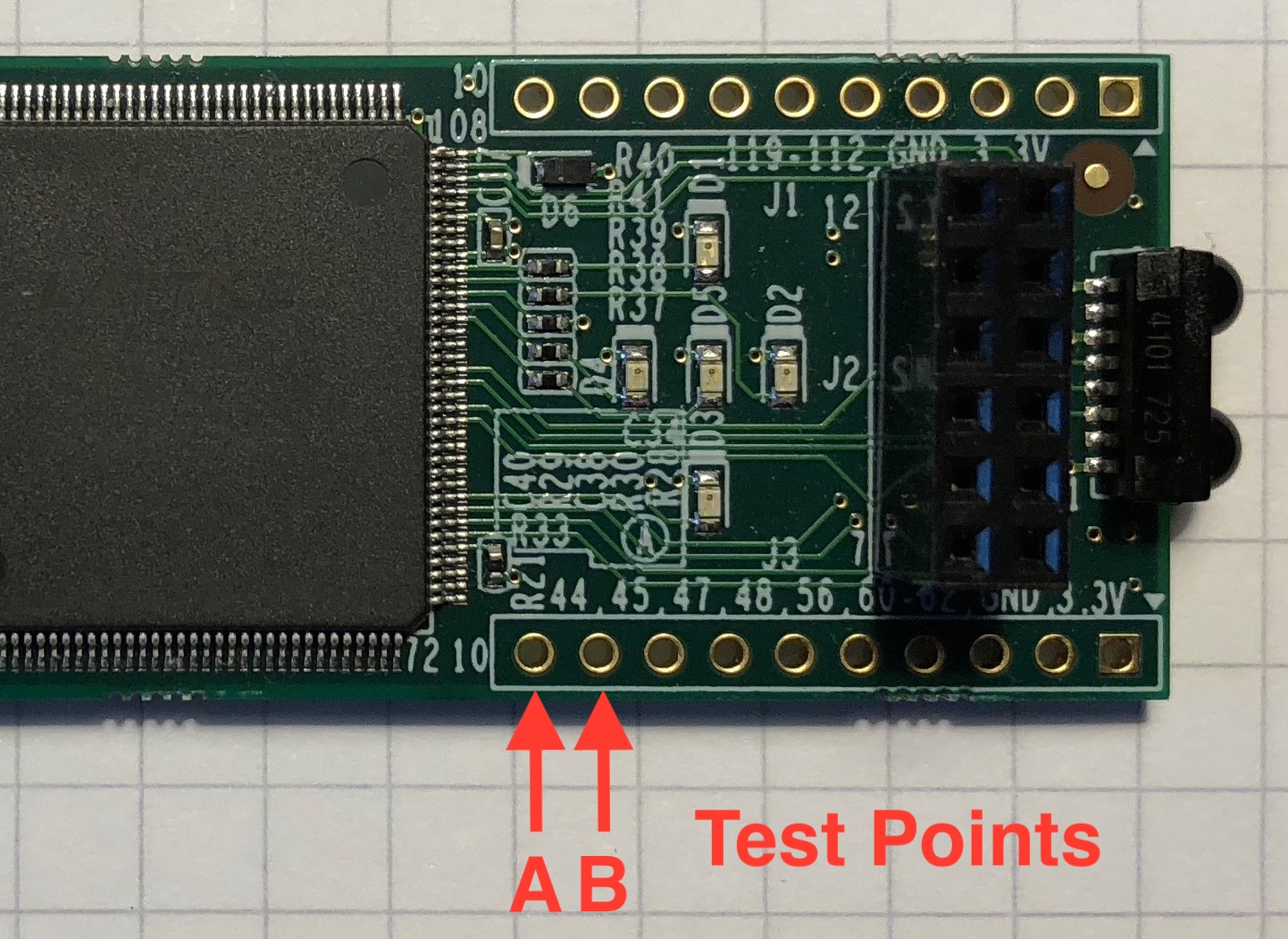
If you have a frequency counter to hand, measure the frequency on test point A: it should be about 6.3MHz. If you prefer something slower, you should find a frequency of about 0.7Hz on test point B.
Hardware Notes
Full schematics of the board are available in the user manual5. Here are some highlights, relevant to our simple project.
FPGA
The FPGA is a iCE40HX-1K in a 144-pin quad flat-pack.
Clock and PLL
A 12MHz clock from a ceramic resonator is provided on pin 21.
This FPGA has a PLL which lets us scale the incoming clock. Arbitrarily, we will try to get a 100MHz system clock, and to do this we need some magic numbers with which we can configure the PLL. Enter icepll:
$ icepll -i 12 -o 100 -m -f pll.v

F_PLLIN:    12.000 MHz (given)
F_PLLOUT:  100.000 MHz (requested)
F_PLLOUT:  100.500 MHz (achieved)

FEEDBACK: SIMPLE
F_PFD:   12.000 MHz
F_VCO:  804.000 MHz

DIVR:  0 (4'b0000)
DIVF: 66 (7'b1000010)
DIVQ:  3 (3'b011)

FILTER_RANGE: 1 (3'b001)

PLL configuration written to: pll.v
As you can see the PLL can’t generate a 100MHz clock, so we will use 100.5MHz instead.
Notice too, that icepll helpfully writes the relevant verilog to a file. Sadly though, that verilog doesn’t use the global clock buffer, so it needs to be tweaked by hand.
LEDs
Four red LEDs are connected to pins 96–99; a green LED is connected to pin 95.
Test points
Dozens of spare IO pins exist, and we use two as test points: pins 44 and 45.
Programming
The board has a FTDI 2232H USB interface which can be used to program flash on the board with iceprog from the IceStorm Tools. However, unless you are prepared to wield a soldering iron, the SRAM in the FPGA can not be programmed directly.
Other peripherals
The manual also contains details of the other peripherals on the board, and, for example, how to use the FTDI chip to talk to a UART on the FPGA. Our needs are more specialized though.
Software Notes
Please remember that you can download all of this from GitHub6.
There are only four small files: a couple of bits of verilog, the pin definitions, and a Makefile.
The main source code
The code is very much as you’d expect. There’s a simple binary counter to reduce the clock frequency to something manageable, then a bit of sequential logic to drive the LEDs.
/*
 * Top module for iCEstick blinky
 *
 * Make circular pattern on red LEDs, flash green LEDs.
 *
 * Generate test signals at 6.28MHz and 0.749Hz.
 */

module top(input CLK
	   , output LED1
	   , output LED2
	   , output LED3
	   , output LED4
	   , output LED5
	   , output TSTA
	   , output TSTB
	   );

   // PLL to get 100.5MHz clock
   wire       sysclk;
   wire       locked;
   pll myPLL (.clock_in(CLK), .global_clock(sysclk), .locked(locked));

   // 27-bit counter: 100.5MHz / 2^27 ~ 0.749Hz
   localparam SYS_CNTR_WIDTH = 27;

   reg [SYS_CNTR_WIDTH-1:0] syscounter;
   always @(posedge sysclk)
     syscounter <= syscounter + 1;

   // test signals on counter
   assign TSTA = syscounter[3];                // 100.5MHz / 2^4 = 6.28MHz
   assign TSTB = syscounter[SYS_CNTR_WIDTH-1]; //                  0.749Hz

   // extract slowest 3-bits...
   reg [2:0]  display;
   assign display[2:0] = syscounter[SYS_CNTR_WIDTH-1:SYS_CNTR_WIDTH-3];

   // .. use slowest to flash green LED,
   assign LED5 = display[2];

   // .. and slightly faster ones to make a spinner
   decode_2to4 myDecoder (.a0(display[0]), .a1(display[1]),
			  .q0(LED1), .q1(LED2), .q2(LED3), .q3(LED4));

endmodule

/*
 * 2-bit to 4-line decode
 *  - positive logic i.e. q0 is high when (a0,a1) == (low,low)
 */
module decode_2to4(input a0, input a1
		   , output q0, output q1, output q2, output q3);

   assign q0 = (~a0) & (~a1);
   assign q1 = ( a0) & (~a1);
   assign q2 = (~a0) & ( a1);
   assign q3 = ( a0) & ( a1);

endmodule
The PLL code
The PLL code is generated by icepll, then edited to use the global buffer for clock distribution.
Technical note TN12517 discusses clocks and PLLs on the iCE40.
/**
 * PLL configuration
 *
 * This Verilog module was generated automatically
 * using the icepll tool from the IceStorm project.
 * Use at your own risk.
 *
 * Subsequent tweaks to use a Global buffer were made
 * by hand.
 *
 * Given input frequency:        12.000 MHz
 * Requested output frequency:  100.000 MHz
 * Achieved output frequency:   100.500 MHz
 */

module pll(
	input  clock_in,
	output global_clock,
	output locked
	);

   wire        g_clock_int;


   SB_PLL40_CORE #(
		.FEEDBACK_PATH("SIMPLE"),
		.DIVR(4'b0000),		// DIVR =  0
		.DIVF(7'b1000010),	// DIVF = 66
		.DIVQ(3'b011),		// DIVQ =  3
		.FILTER_RANGE(3'b001)	// FILTER_RANGE = 1
	) uut (
		.LOCK(locked),
		.RESETB(1'b1),
		.BYPASS(1'b0),
		.REFERENCECLK(clock_in),
	        .PLLOUTGLOBAL(g_clock_int)
		);

   SB_GB sbGlobalBuffer_inst( .USER_SIGNAL_TO_GLOBAL_BUFFER(g_clock_int)
			   , .GLOBAL_BUFFER_OUTPUT(global_clock) );

endmodule
Makefile
Most of the rules are shared across different dev. boards: we need only to specify the FPGA and the programming software:
ARACHNE_DEVICE = 1k
PACKAGE        = tq144

ICETIME_DEVICE = hx1k

PROG_BIN       = iceprog

include ../std.mk
Pin summary
Finally, we need to tell the software which pins are associated with the signals:
$ cat pins.pcf
set_io LED1 99
set_io LED2 98
set_io LED3 97
set_io LED4 96
set_io LED5 95
set_io CLK  21
set_io TSTA 44
set_io TSTB 45
References
- 1. http://ice40-blinky.html
- 2. http://www.latticesemi.com/icestick
- 3. ./ice40-toolchain.html
- 4. https://en.wikipedia.org/wiki/Blinkenlights
- 5. http://www.latticesemi.com/view_document?document_id=50701
- 6. https://github.com/mjoldfield/ice40-blinky
- 7. http://www.latticesemi.com/~/media/LatticeSemi/Documents/ApplicationNotes/IK/iCE40sysCLOCKPLLDesignandUsageGuide.pdf?document_id=47778
![[ Atom Feed ]](../../atom.png "Atom Feed")